
Electronics Design Workflow
Learn how to move from an idea to a working electronics project through requirements, prototype testing, schematic design, PCB layout, assembly, testing, and documentation.
1. What you will learn
2. Workflow references
3. Learning modules
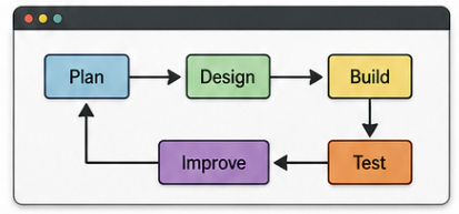
Work through these modules in order. Each module follows a practical electronics design workflow that helps you avoid rebuilds, wrong parts, wiring mistakes, and unreliable prototypes.
1 Define the goal Write what the project needs to do and what constraints matter.
A good project starts with a clear goal. Before choosing parts or drawing a schematic, define what the device should do, how it will be powered, where it will be used, and what limits matter. This prevents the project from growing randomly while you build it.
Write the goal in simple terms. For example: “Build a small display device that shows live PC values over USB and fits into a desktop enclosure.” This is much clearer than only saying “build a display project.”
- Define the function: What should the project measure, control, display, or automate?
- Define the inputs: Buttons, sensors, serial data, wireless data, or user settings.
- Define the outputs: LEDs, displays, motors, relays, sound, or data logging.
- Define the limits: Size, power source, budget, heat, runtime, connector access, and safety.
A useful rule is: if you cannot describe the project in a few clear sentences, it is not ready for schematic or PCB work yet.
2 Prototype the unknowns Test the display, sensor, power stage, or communication before PCB design.
The purpose of a prototype is not to build the final device. The purpose is to test the risky or unknown parts before you invest time in a permanent build. This can include a new display, a sensor, a communication interface, a battery circuit, or a high-current output stage.
Start with the smallest possible test. If the project uses an ESP32, a TFT display, and serial data from a PC, do not test everything at once. First run the display example. Then test serial communication. Then combine both parts.
- Test one function at a time: Display, sensor, power, button, communication, or output stage.
- Use example code first: Confirm the hardware works before writing the full firmware.
- Measure early: Check voltage rails, current draw, logic levels, and signal activity.
- Keep notes: Save working pinouts, library versions, settings, and test results.
A prototype is successful when it answers a clear question, such as “Can this display refresh fast enough?” or “Does this sensor work reliably with this cable length?”
3 Create the schematic Use readable component names, connector names, and net labels.
The schematic is the electrical plan of the project. It should show how every part is connected, which voltage rails are used, where signals go, and how external modules or connectors are wired. A clean schematic makes PCB layout, debugging, and future changes much easier.
Use clear names instead of relying only on wires crossing the page. Important signals such as 5V, 3V3, GND, SDA, SCL, MOSI, MISO, SCK, CS, BUTTON, LED_DATA, and PWM_OUT should be easy to find.
- Name connectors clearly: Use names like DISPLAY, POWER_IN, SENSOR, BUTTONS, or LED_STRIP.
- Label power rails: Keep 5 V, 3.3 V, battery voltage, and ground easy to identify.
- Add protection where needed: Consider fuses, reverse-polarity protection, flyback diodes, and current-limiting resistors.
- Check every pin: Compare the schematic pinout with the real module, datasheet, or footprint.
A good schematic should be understandable even months later. If you need to explain every connection from memory, the schematic is not clear enough yet.
4 Layout the PCB Place connectors logically and route power and ground carefully.
PCB layout turns the schematic into a physical board. Component placement is usually more important than routing. Place connectors where the cables need to exit, place buttons where the user can reach them, and place displays or LEDs where they align with the enclosure.
Power and ground routing should be planned early. High-current paths should be short and wide. Sensitive signals should not be routed next to noisy motor, LED, relay, or switching-converter traces if it can be avoided.
- Place first, route second: A good placement makes routing easier and cleaner.
- Use wider traces for power: LED strips, motors, displays, and regulators need stronger power paths.
- Keep decoupling close: Place capacitors near IC power pins and module supply inputs.
- Check connector orientation: Make sure pin 1, polarity, and cable direction match the real build.
- Leave mechanical clearance: Screws, standoffs, case walls, displays, and cables need physical space.
A clean PCB layout is not only about looking nice. It improves reliability, makes assembly easier, and reduces debugging time.
5 Review before ordering Check footprints, pin orientation, mounting holes, and mechanical fit.
The final review is the last chance to catch mistakes before the board is manufactured. Many PCB problems are not caused by complex electronics, but by wrong footprints, reversed connectors, missing pull resistors, incorrect pin mapping, or parts that do not physically fit.
Do not review only on the screen. Print the board layout at 1:1 scale if possible and place real components on the paper. This quickly reveals wrong connector spacing, display alignment issues, button position problems, or mounting hole mistakes.
- Check footprints: Confirm pad size, pitch, package type, and orientation.
- Check pin 1: ICs, connectors, displays, and modules must match the real part orientation.
- Check power rails: Verify voltage direction, regulator input/output, and polarity.
- Check mechanical fit: Mounting holes, enclosure walls, USB ports, displays, and connectors must align.
- Run design checks: Use ERC/DRC tools and inspect every warning instead of ignoring them.
A careful review can save weeks of waiting, reordering, and rebuilding. Most PCB mistakes are easier to prevent than to repair.
6 Document the project Save wiring diagrams, code, photos, notes, and version changes.
Documentation turns a working project into something you can repair, improve, share, or rebuild later. Good documentation does not need to be complicated, but it should capture the information that would otherwise be forgotten.
Save the schematic, PCB files, exported Gerbers, bill of materials, firmware, wiring photos, enclosure dimensions, test notes, and known issues. Also document what changed between versions, especially if you fix a wiring error or replace a component.
- Save the final pinout: Include controller pins, connector pins, and signal names.
- Keep a BOM: List components, values, quantities, and useful part links.
- Take photos: Photograph wiring, solder joints, connector orientation, and final assembly.
- Record test results: Note supply voltage, current draw, temperature, and firmware version.
- Track versions: Clearly separate prototype, revision 1, revision 2, and final files.
Good documentation is especially useful for tutorials. It helps other people follow the project and helps you avoid giving incomplete or confusing build instructions.
4. Project connections
These examples show where the topic appears in practical ElektroBox builds.
5. Common mistakes
Skipping basic checks
Always verify power, ground, polarity, pin assignment, and the simplest possible test case first.
Changing too many things at once
Change one variable, test again, and document the result. This keeps debugging controlled.
Ignoring component limits
Check voltage, current, heat, pin limits, and power ratings before assuming a circuit is safe.
Final takeaway
A good workflow reduces rebuilds. Most mistakes can be caught before ordering parts or publishing the final project.